-
Mitalee Parikh authoredMitalee Parikh authored

#Project Development This part of the course was longer for me than a couple of weeks. I managed to find access to a lab - FabLab UAE and am very thankful to Hashim for letting me use the resources of the Lab, and Steven for setting this up for me.
Page Summary
- Project Management
- Tracking progress
- Development
- Important and interesting links
- Project Management
Murphy's Law - everything that can go wrong will go wrong. This has happened many a times for me in respect to FabAcademy.
Triage - I have some trouble with this. As I get easily distracted and go into the depth of things without zooming out in time to finish the assignments.
Documentation during development - Fighting procrastination to get better with this.
Demand- vs supply-side time management - Generally I used this for the last 2-3 weeks before the final project submission deadline.
Spiral development, DevOps - This is my favourite. I have started using this in my design practice and various other aspects of life.
Serial vs parallel tasks - I do both depending on the task, the time and the surrounding contexts.
System integration - getting better and better at this with time, documenting this is very difficult because of non compartmentalisation.
Finish quality - I believe in using materials in an honest way to hero their intrinsic properties and not hide them under aesthetic finishes. This makes the underlying parts neat and organised automatically.
- Tracking progress
What tasks have been completed, and what tasks remain?
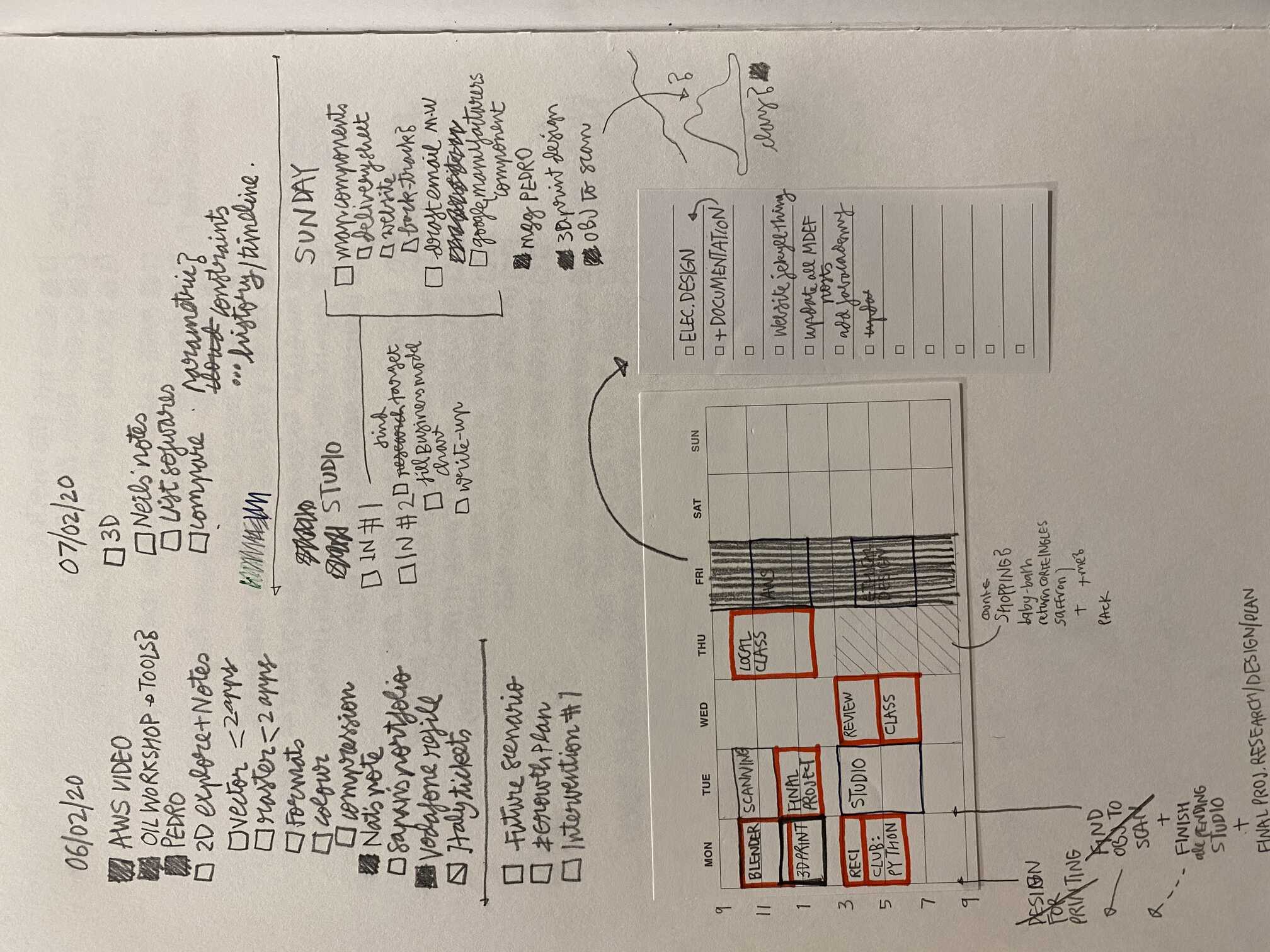
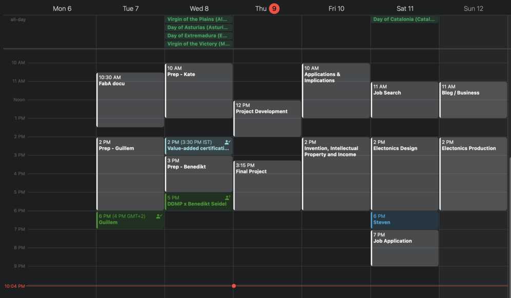
I kept a record of this by making a to-do list every week in my notebook and then assigning time for each task in my calendar. Here are some pictures of my to-dos:
What's working? What's not?
The OLED screen I borrowed from the lab, stopped working after I tried it with an Arduino Uno. I'm not sure what was wrong, but I checked every connection with a multimeter. I tried an I2C scanner detector but it still did not detect the device. I also tried it with a different programming board, and a I2C LCD screen with the same board. But after testing each connecting part, something in the OLED did not work. So finally, I got a new one.
The laser cutter I used at the Lab - a Universal Laser system, had a different kerf in the x-axis and the y-axis. I tried many different combinations of settings and materials. But still could not figure out how to fix this. Eventually I offset my tongue and groove joints different in X- and Y- directions.
I designed and made my PCB using an ATtiny44 microcontroller. Early on I figured that all the different libraries I would need to work the DHT11 and the OLED would not fit in the 4k storage space. So I desoldered the 44 and used an ATtiny84, so that nothing would change but the microcontroller. Eventually I discovered the tiny libraries for OLED and DHT - optimal versions of the full libraries and turned out the code used only 4136 bytes of storage space.
I made the first layout of the PCB trying to make it as compact as possible by keeping parts close together and traces more optimised on space. Eventually, I changed the layout of the header pins that connect to all different input/ out puts and matched them to their physical location on the machine. This resulted in a much bigger PCB but a very neat layout of all the wiring. I planned it such that the wiring would neatly stretch on the side of the machine, but Neil suggested using a cable manager instead.
I also wanted to add a mobile application to control the machine instead of the physical regulators and switches as the last spiral development cycle including a wifi module.
What have you learned?
Through this project I learnt the most in electronics design and programming. The process of 'How to design a PCB from scratch for what you want the thing to do' as described in the weekly documentation was the most empowering.
- Development
Process
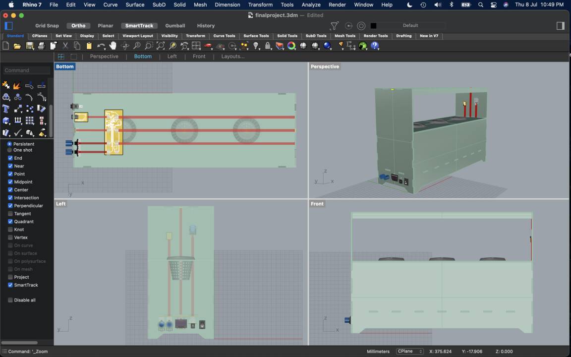
- First I started by making a CAD model in Rhino. I explored multiple forms.
 Since I need to make as many parts as possible in the lab instead of buying parts, I modify the design to make it less curved and simpler to cut and assemble.
Designing the electronics:
####Inputs to include:
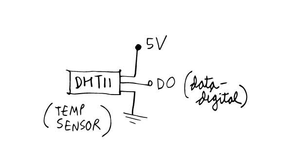
- DHT11 - temperature and humidity sensor
- Phototransistor - to measure ambient light intensity
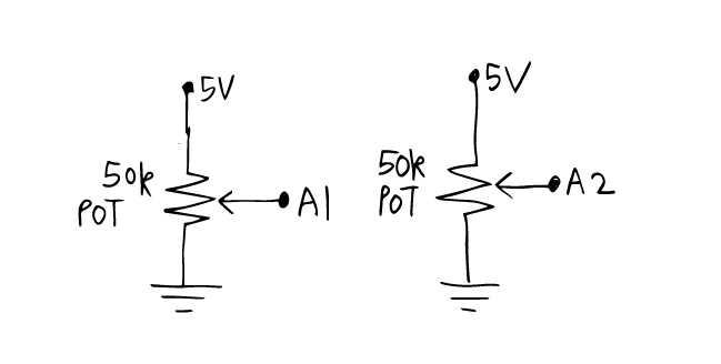
- Potentiometer / variable resistance - to control flow of water through pump
- Potentiometer / variable resistance - to control grow light intensity
- Toggle switch for power on/off
####Outputs are:
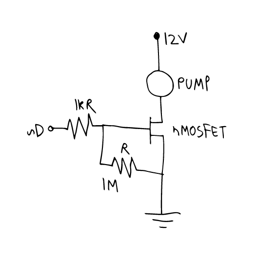
- 12V DC pump to pump water through a sprinkler system
- 12V DC growth light strip with 3:1 RB 5050SMD LEDs
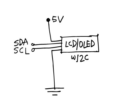
- SSD1306 OLED screen with I2C
With the help my instructor Steven, I developed a basic scheme for the electronics.
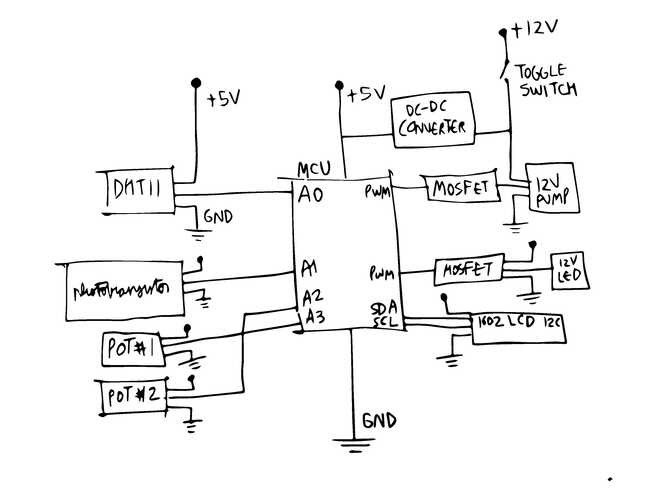
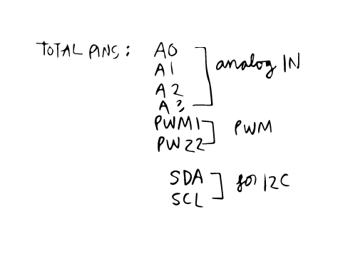
Also counting the pins required for each sensor and actuator:
Since I am not in the lab, I need to order some components myself. I start making a Bill of Materials for the project electronics:
Next, I started making a schematic according to the sketch, connecting each component to V, GND and respective pins.
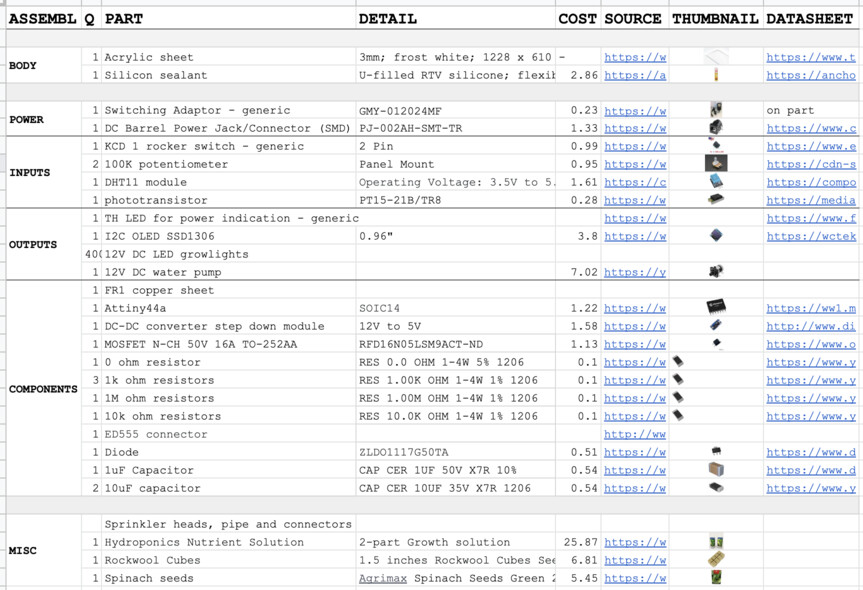
12V DC-DC converter to 5V
The DC-DC converter will have connections based on the datasheet...
I'm connecting a toggle switch to the converter, which will be the power on/off switch for the user
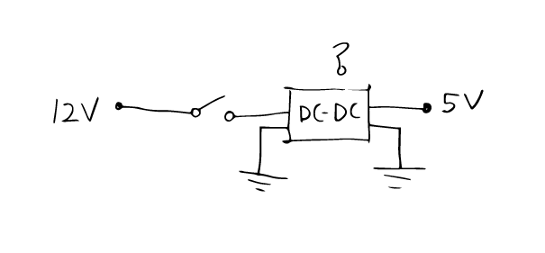
I'm also adding a red SMD LED as a power indicator.
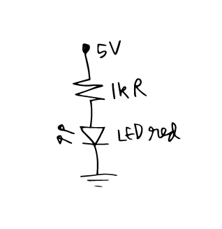
Phototransistor has two options of circuits, according to this guide.
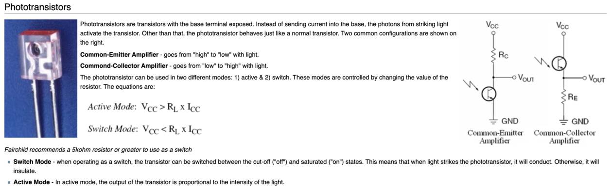
I use the Phototransistor in active mode - meaning the output of the transistor is proportional to the intensity of the light.
![]()
The potentiometers have 3 pins - one for power, one GND and third data that connects to the MCU.
The temperature and humidity sensor DHT11 has 3 pins - 5V power, GND and data which connects to a digital pin of the MCU.
Ref: Introduction to DHT11
I use an OLED SSD1306 with I2C to make serial communication easier and use less pins on the MCU, only SDA and SCL.
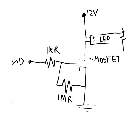
A 12V DC water pump is connected to the MCU with a n-channel MOSFET so I can control the flow of water using Pulse Width Modulation.
Similarly the 12V DC LED growlight strip is connected to the MCU with a n-channel MOSFET so I can control the light intensity. These come in different ratios of red-blue lights. I plan to use one with 3:1 meant for leafy plants.
Next, I use KiCAD to put all these schematics together and begin to design my PCB.
While making the schematic I realise not all sensors and actuators need to be on the PCB itself, some like the pump and the LED and the DHT11 need to be at a different physical location on the designed box, so I need to add header pins and connect them using wires later.
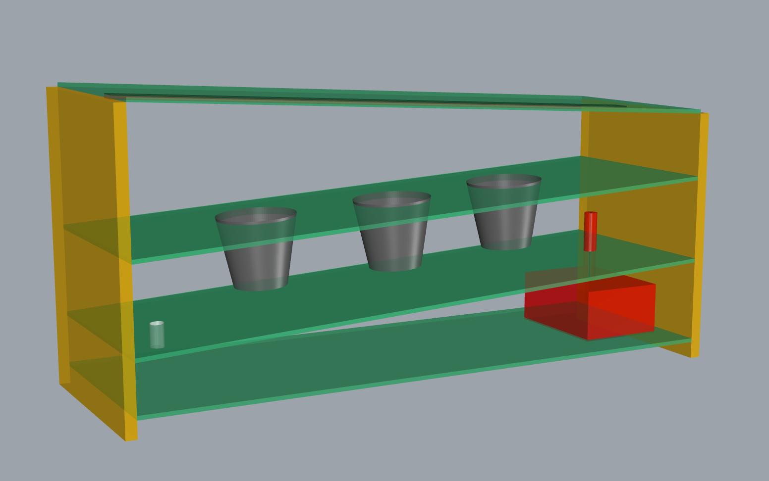
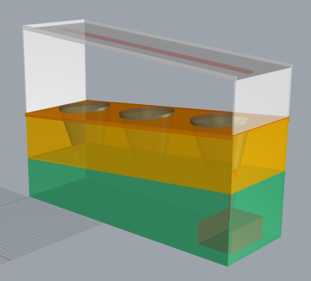
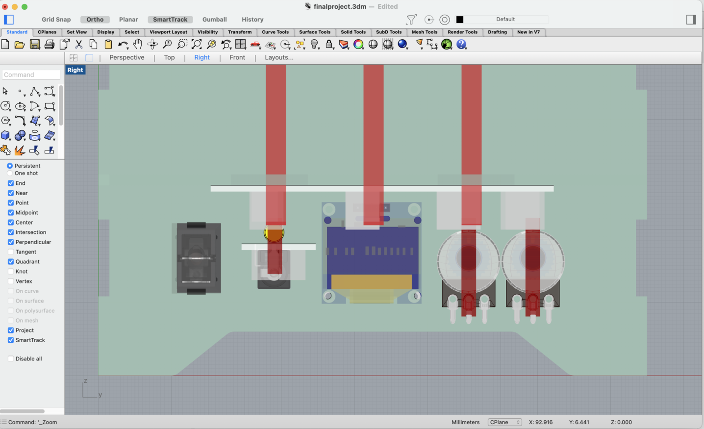
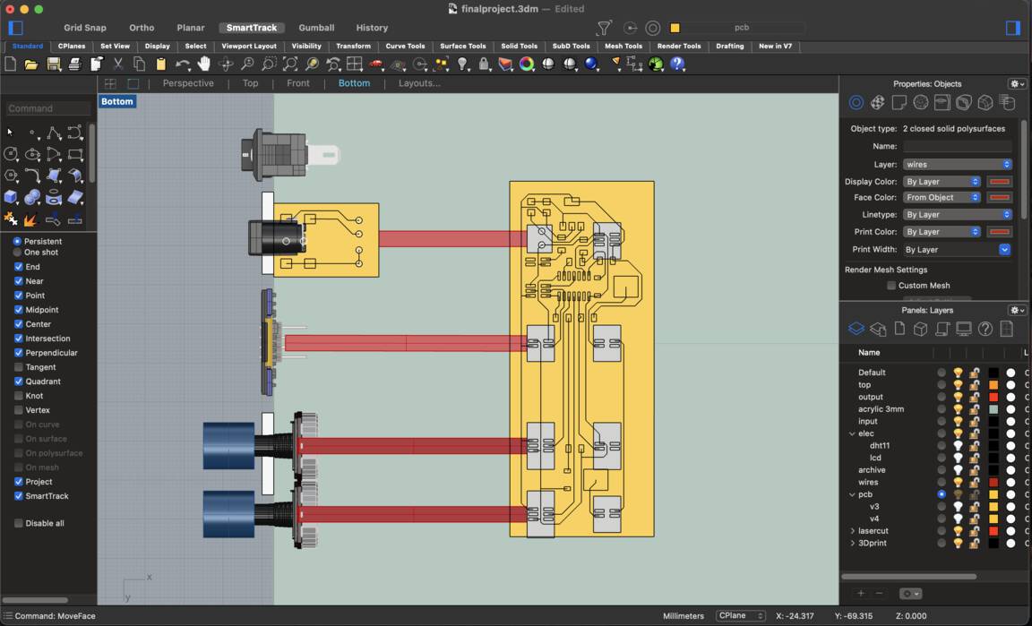
To clarify this, I begin modifying my 3D CAD model on Rhino.
And then redo the schematic.
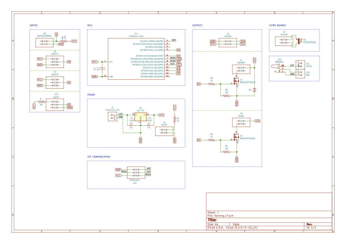
Next, I generate the Netlist and load it in the pcbnew of KiCAD. I arrange all header pins in a linear fashion so that they do not get jumbled and don't cross each other like in the model.
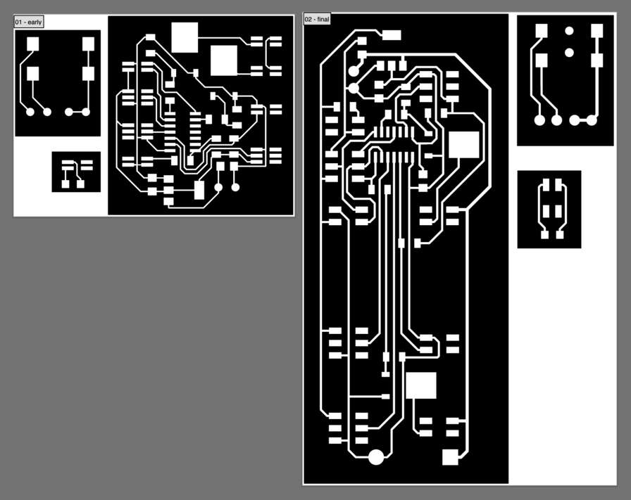
Some failed attempts:

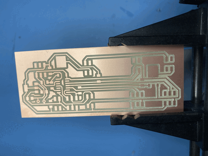
After about 7 revisions, changing minor details, I made
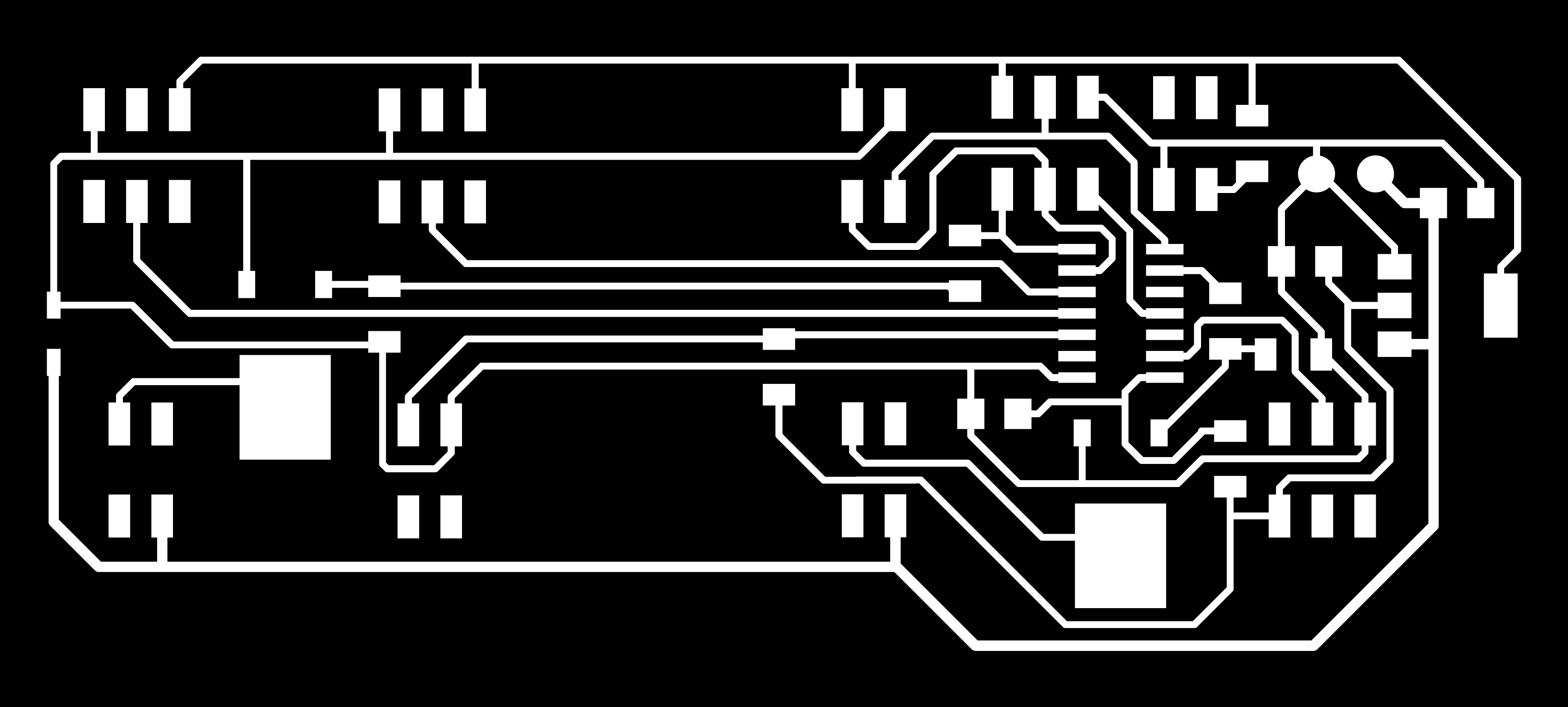
Here are the final design files for the board:
Schematic v7
Traces png
Outline png, containing the holes too.
####Things to do next: Milling prcoess Soldering Components Testing board Connecting all inputs and outputs
####Milling the PCB
####Soldering components
After making a 'shopping list' I gathered all components. Most of them were available from the Lab (FabLAb UAE).

As good standard practice, I soldered all components from left to right and top to bottom. Starting with the microcontroller, then smaller components like resistors, capacitors, then the larger mosfets and DC-DC voltage regulator and all the header pins in the end.
####Testing board
I was missing a diode. Since this wasn't in the lab, I used a TH component, cut legs and soldered it directly onto the copper tracks. It was a little delicate, but it worked. I had to make sure it was connected in reverse to save the DC outputs from burning.
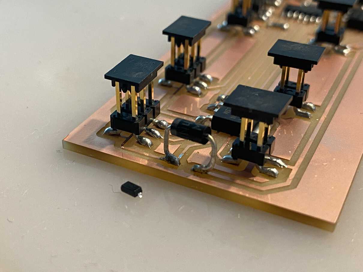
I also cleaned up the board for copper shards and tested all connections using a multimeter. Beeping all VCC, GND connections to themselves and measuring resistance across al resistors.
####Wires and wiring
I used ribbon cable and cut them to custom lengths according to the 3D model. And hammered on header pins with 2x rows instead of 1, to make the connections sturdier.
####Programming: I will use the FabISP I made in Electronics Production week as a programmer to program my farming board with all the inputs and outputs.
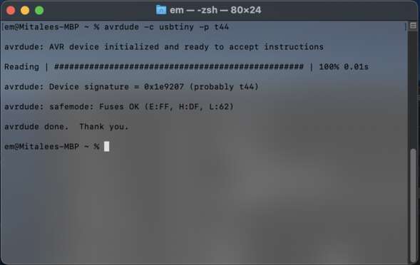
AVRDUDE is a utility to download/upload/manipulate the ROM and EEPROM contents of AVR microcontrollers using the in-system programming technique (ISP).
- Connect the new board with a ribbon cable to the FabISP programmer through a compatible USB adaptor.
Check the orientation of the cables is on correct order. VCC of the FabISP matches the VCC of the target board(mine with ATtiny44)
Check System Report > Hardware> USB, should detect the USBtinyISP.
Next in a terminal window,
avrdude -c usbtiny -p t44It should show that the device is initialized and show a signature.
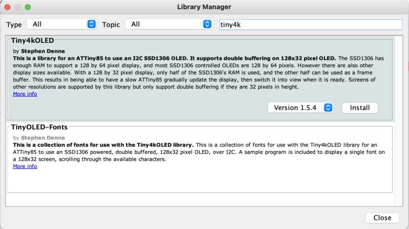
Next, I will start adding the i/o one by one starting with the OLED so I can use it as a display for troubleshooting along the way. Since I'm using a Attiny44 with 4k memory, I will use the minimal versions of OLED and DHT libraries to make enough space for the rest of the components.
- Install OLED library from https://github.com/datacute/Tiny4kOLED which is a Library for an ATTiny85 to use an SSD1306 powered, double buffered, 128x32 pixel OLED, over I2C.
Open Arduino IDE, in Tools > Board Manager, add the https://github.com/technoblogy/tiny-i2c in additional boards URLs.
Sketch > Include Library > Manage Librarries, select Tiny4kOLED and install.
3D printing
Knobs for potentiometers: [3D model]