-
Mitalee Parikh authoredMitalee Parikh authored

Electronics production
This week I made an in-circuit programmer- the FabISP.
FabISP
Making toolpaths
I downloaded the png files for the traces and the interior. I used FabModules to create toolpaths.
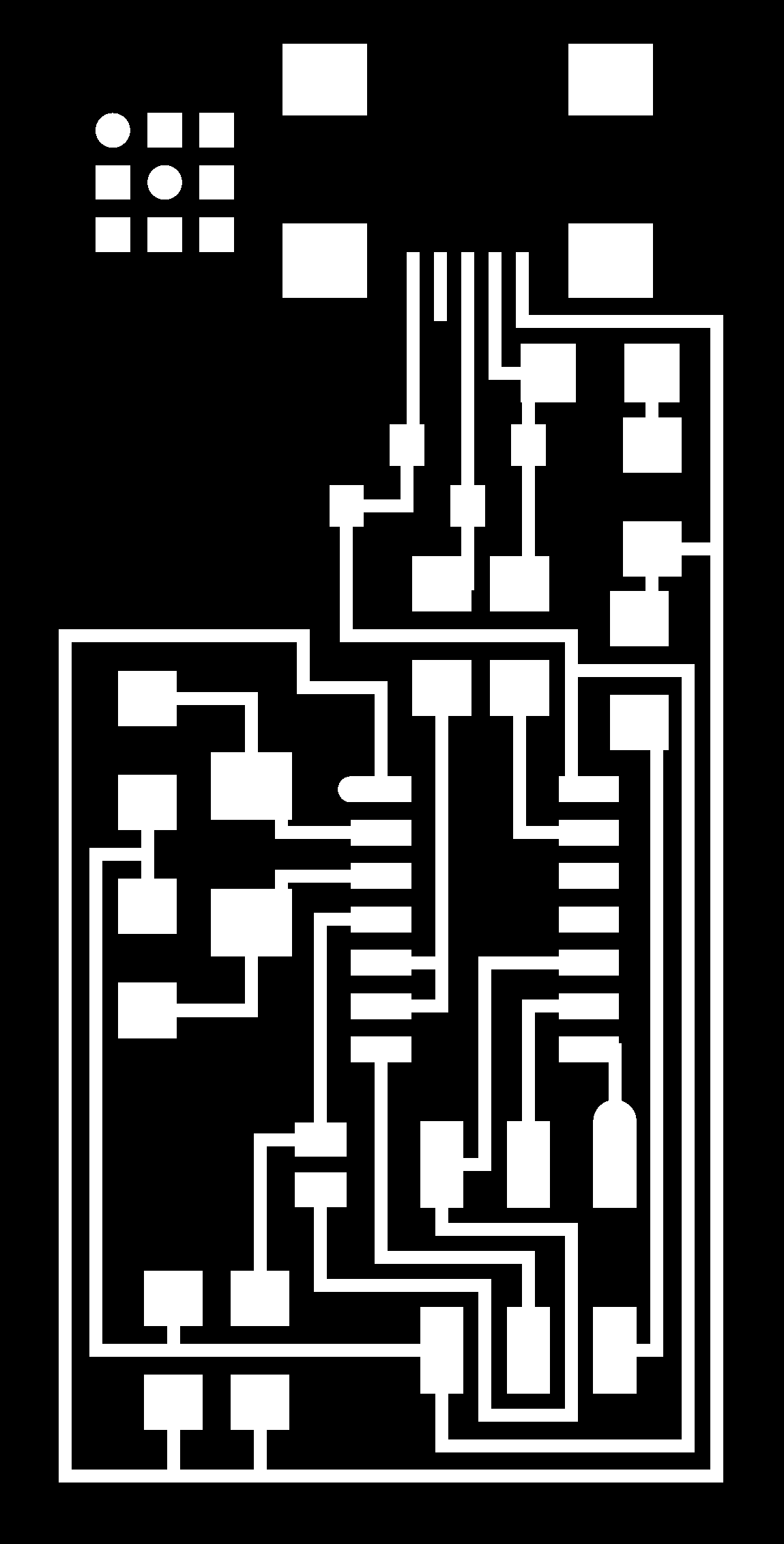
Traces
The major settings for cutting traces: Input image as .png
Output file as .rml
Output file as .rml
Machine: Roland SRM-20
Speed: 3.5mm/s as I was using a new endmill
Origin X,Y,Z as 0,0,0 to match the origin set in the machine locally
Tool diameter 1/64"
Offset paths 4, to clean area around the traces but not very time consuming
Overlap 50%, Overlapping the tool paths by 50% of the tool diameter
Cut depth 0.1mm to clean the top copper layer through it's thickness


Interior
Settings for cutting the outline:
Input image as .png
Output file as .rml
Machine: Roland SRM-20
Speed: 0.5mm/s
Material depth 1.7mm, equal to the one-sided FR1 board used
Cut depth 0.5mm, cuts the outline 4 times going 0.5mm deeper with every loop
Origin X,Y,Z as 0,0,0 to match the origin set in the machine locally and match the traces file
Tool diameter 1/32"
Offset paths 1, to cut the board from the material
Milling the board
Cleaned a small piece of one-sided FR1 board with rubbing alcohol.
Stuck it using a double-sided tape on an MDF base we have pre-installed at the lab, that is levelled periodically.
Installed a 1/64" tool
Set the X and Y origin on the bottom left corner of the board.
Brought the Z really close to the top of the surface. Loosened the collet and let the bit touch the surface completely. Set the Z origin here.
Lifted the Z, loaded the rml traces file and start cutting. Everything seemed fine. I could see the tool cut though the copper. It took about 15 minutes to cut the whole file.
Later, I lifted the Z, changed the tool to the 1/32" endmill to cut the interior file. I set the Z origin again exactly as before. Keeping in mind not to change the X and Y origin. Started cutting the file. Got it done on the first try. I unattached the board using a scraper.


Soldering Components
Gathering Components
Edu showed us the best way to do this was to make a shopping list, collect components and stick them on using tape. Later, we update the inventory sheet to keep count in the lab.
A list of all the needed components:
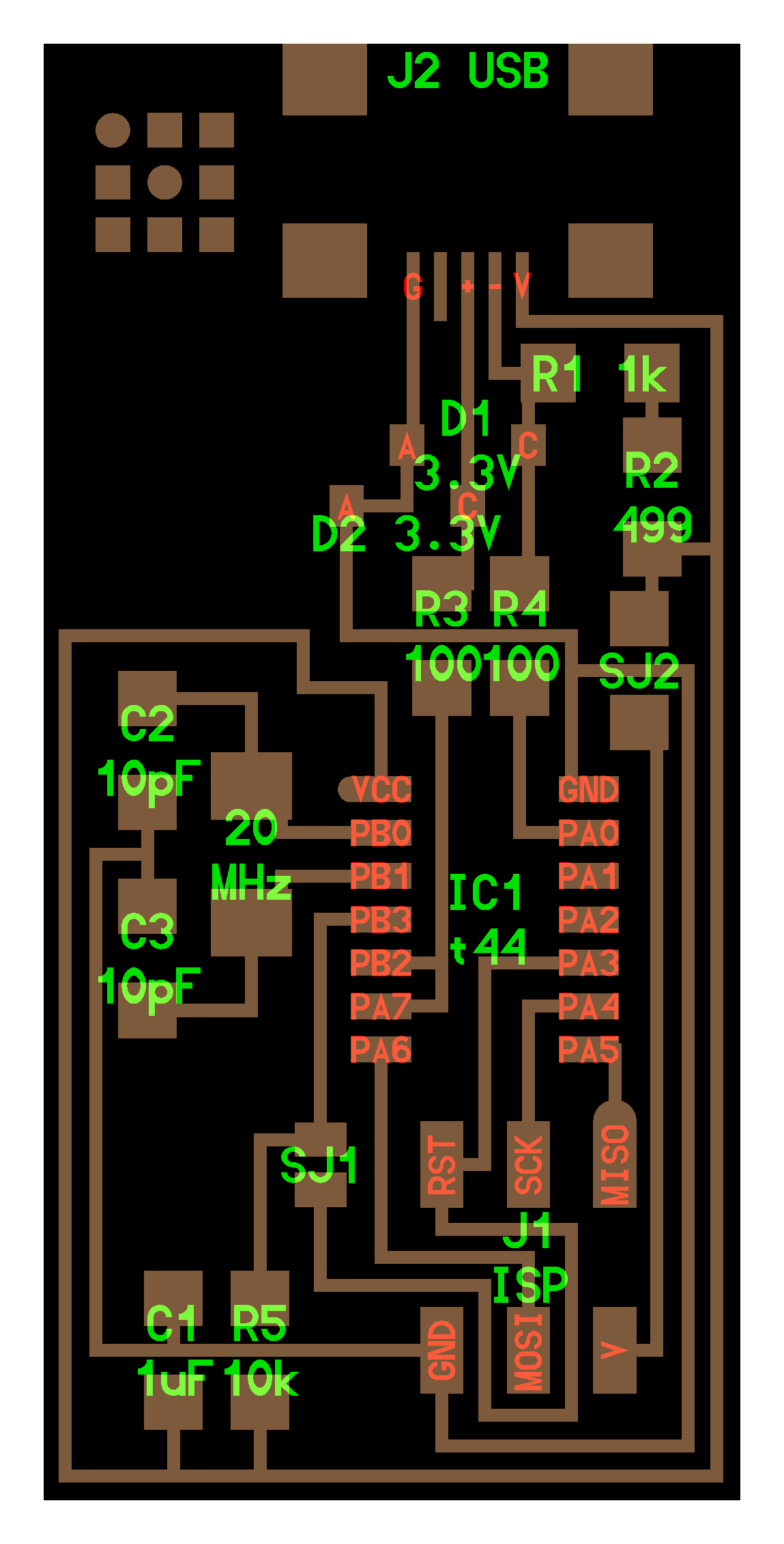
1 x ATtiny44 (Ict44)
1 x 6-pin(2x3) header (J1 ISP)
1 x MiniUSB header (J2 USB)
1 x 20MHz Crystal (20MHz)
1 x 1uF Capacitor (C1)
2 x 10pF Capacitor (C2,C3)
2 x 3.3v Zener Diodes (D1,D2)
1 x 1kΩ Resistor (R1)
1 x 499Ω resistor (R2)
1 x 100Ω resistor (R3,R4)
1 x 10kΩ resistor (R5)
2 x 0Ω Resistor (SJ1, SJ2)

The solding set-up
Tools that I need to solder the components on the board: A schematic diagram that shows what components goes where.
The components, gathered on the list. A soldering iron - I used a Weller WES51 with temperature control. Set it to 750F, not too hot, not too slow. A wet sponge, to clean the tip of the iron. Solder wire, Kester without a flux co. A anti-static curved tweezer to place down components accurately. A copper braid for desoldering excess solder. A table-top light, a silicon base to hold the board stationary, and a fan to remove fumes.
Soldering order
I started from the complex to the simple, then top to bottom. I soldered the microcontroller first, matched the orientation from from the data sheet. Second, I soldered the MiniUSB, since, it had very tiny trace connections. The zener diodes, have polarities. i soldered them next. Oscar taught me how the way to remember their direction, the electric symbol has a line that corresponds to the Cathode. Similarly, the component is marked with a line in its cathode side. Polarity symbol The rest of the components don't have any polarities, so I soldered them from top to bottom inside-out in this order: R1>R2>R3>R4>SJ2>20MHz>C2>C3>SJ1>R5>C1 and the J1 header in the end, because it had comparatively larger feet.
Checking connections
I visually checked the board under a lens to check no traces or solders touched each other. Then using a multimeter setting with no resistance, I connected all pin legs to where the traces connected using the schematic diagram. And checked that all beeped, suggesting there was no short. I cleaned the board again, using some rubbing alcohol. This is how my finished board looks: 