-
Mitalee Parikh authoredMitalee Parikh authored

#Electronics Production This week is about learning how to fabricate a PCB.
Page Summary
- Summary
- PCB fabrication
- Assembling the board
- Testing and programming
- Important and interesting links
- Summary
There a some different options of in-system programmers in the FabAcademy notes. In the AVR family, there are boards based on the the ATtiny45, ATtiny44 and ATmega16U2.
I review all options, and decide to make the ISP based on Brian's design because it seemed simple and straight-forward, and a good one to start with because it has ample documentation. It is called the FabTinyISP.
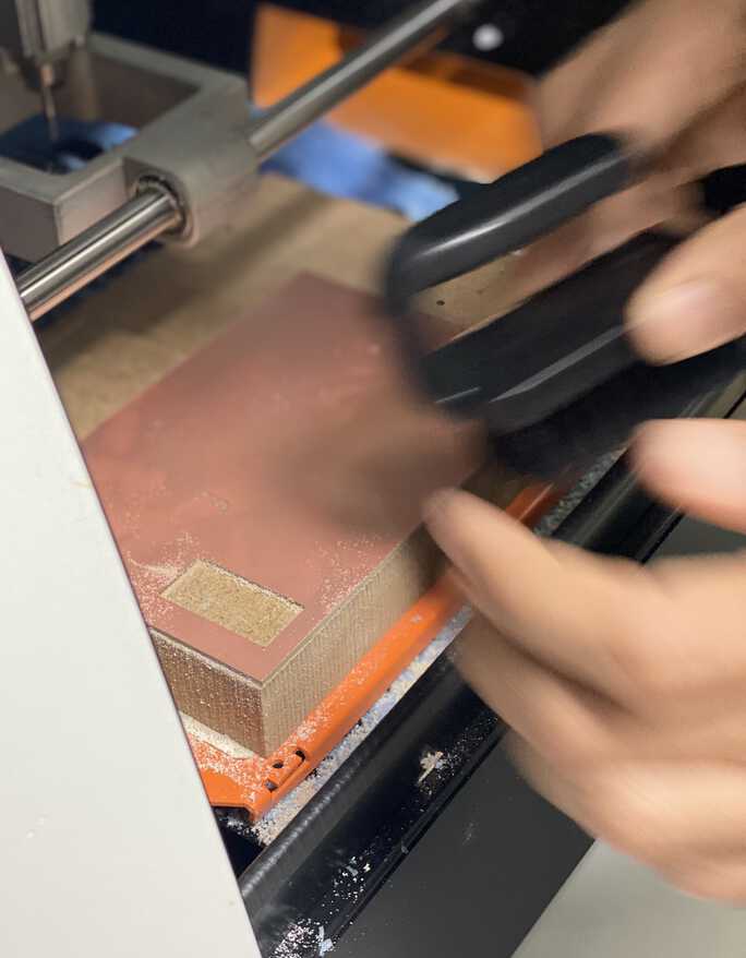
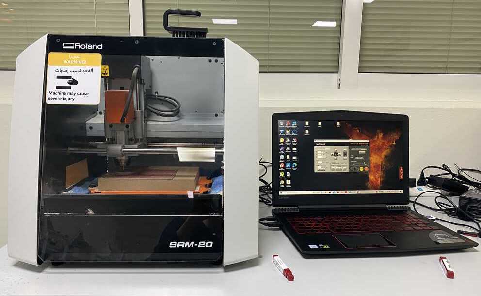
I used the facilities in FabLab UAE to fabricate the ISP with a Roland SRM-20 milling machine.
I use a double sided FR1 board to mill the ISP, because the lab is out of stock of single-sided ones that are not locally available.
An in-system programmer is basically serial programming that allows programming and reprogramming of microcontrollers, soldered on a target Printed Circuit Board. This week is about learning both, making the PCB from scratch and programming the microcontroller on it to become a programmer itself.
- PCB fabrication Workflow
The PCB workflow basically consists of making png traces/outlines from a design file, or using existing ones > creating toolpaths > prepping a milling machine > loading a copper sheet and endmill > setting origin on machine > milling and then cleaning to solder components before stuffing and testing the board.
Create toolpaths
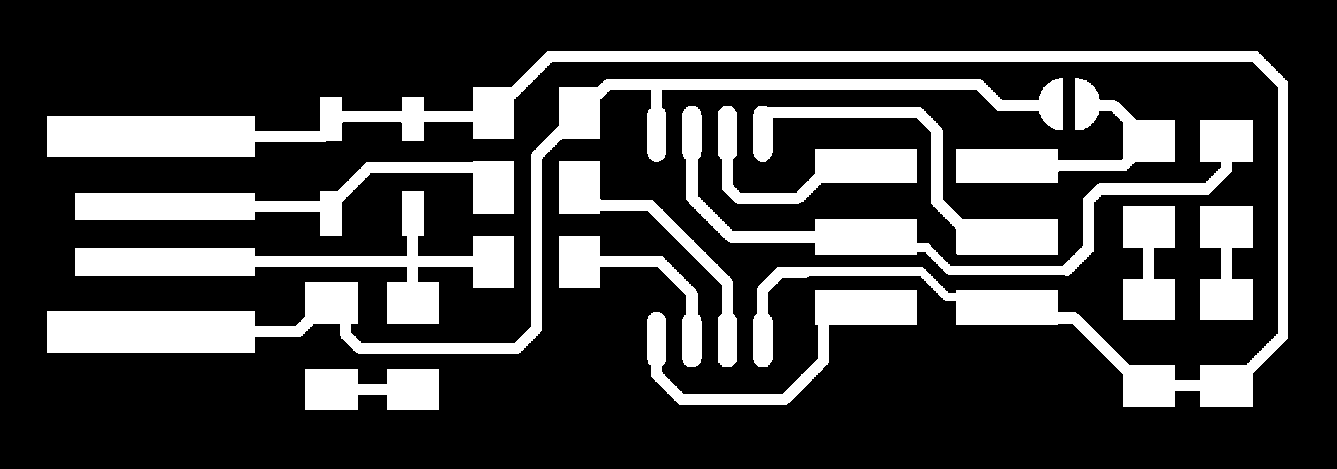
First step is to download the design files for the traces and the outline of FabTinyISP from Brian's documentation page.
The traces are the thin pipelines that connect the footprints of components.
Traces (1000dpi)
The outline is the outer boundary to be cut. Sometimes it also includes through-holes to be made in the PCBs.
Outline (1000dpi)

It is important to note that both these images are at 1000 dpi resolution in png format.
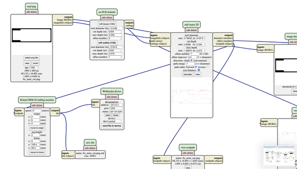
Next, these png images need to be converted to tool-paths for CNC machines to follow. Fabmodules and Mods both, developed by the Fab community can be used to make the tool-paths. They run in the browser.
I first use Mods.
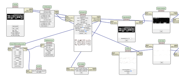
But it shows me unclear toolpaths with default settings, for both the traces and the outlines. With random dots being detected arounf the traces.


I'm not sure why these errors occured. I try using FabModules with the same files and same settings. And it works perfectly. So I guess Mods has a different way to read these files.
Characterising design rules for your PCB production process
- Select input format: png (same as the file downloaded)
- Select the traces file from your directory
- The input section on the rights shows the meta info of the image. Check the resolution is 1000 dpi and the overall size. The - image is 1:1 so the PCB will be the same size as mentioned here.
- Select output format: rml (depends on the machine you use; Roland machines use rml)
- Select machine from the dropdown: SRM-20 (I'm using this at the lab)
- Speed: 4 mm/s Standard speed used with a 1/64in endmill
- x0, y0, z0 all 0 this makes the cutting start exactly where you set the origin on the machine
- zjog: 2 mm is the distance the endmill travels in z direction when it lifts up to move in the air to another xy coordinate
- xhome, yhome, zhome are the coordinates the endmill moves to at the end of the job, i leave this empty so it take the default - value of the machine.
- Select process: PCB traces (1/64) this basically fills in default values for the standard trace milling process
- Direction: climb here is a diagram that explains climb vs conventional cutting
- Cut depth: 0.1mm to cut through the upper layer of the FR1 boards
- Tool diameter: 0.4 mm (=1/64 in)
- Number of offsets: 4 this is the number of paths around the traces, if its too little soldering components is difficult, if it - too much, it takes a long time to mill, 4 is just enough (-1 to remove everything completely)
- Offset overlap: 50% The overlap between two paths, to ensure no material is left with error

With these settings, I calculate the toolpaths for the traces and save the rml file.
Making the outline has the same process except the following changes:
- Select the outline file from your directory
- Select process: PCB outline (1/32) because outline is milled with a different endmill
- Cut depth: 0.6mm keep this a bit smaller than the tool diameter, so it doesn't break the bit
- Tool diameter: 0.8 mm (=1/32 in)
- Stock thickness: 1.7 mm Thickness of the FR1 stock measured with a calliper
- Number of offsets: 1 The outline can be cut with just 1 path around the board
Since the cut depth is 0.6, to cut through the 1.7 mm stock, it will run the path 3 times till it cuts through the entire thickness of the stock. This can be seen when you calculate the toolpath.

Here are the toolpath files for traces and outline.
Milling the board
After saving the toolpaths, next step is to prep the machine for milling.
On the left bottom corner, fix the FR1 board with a double-sided adhesive tape.