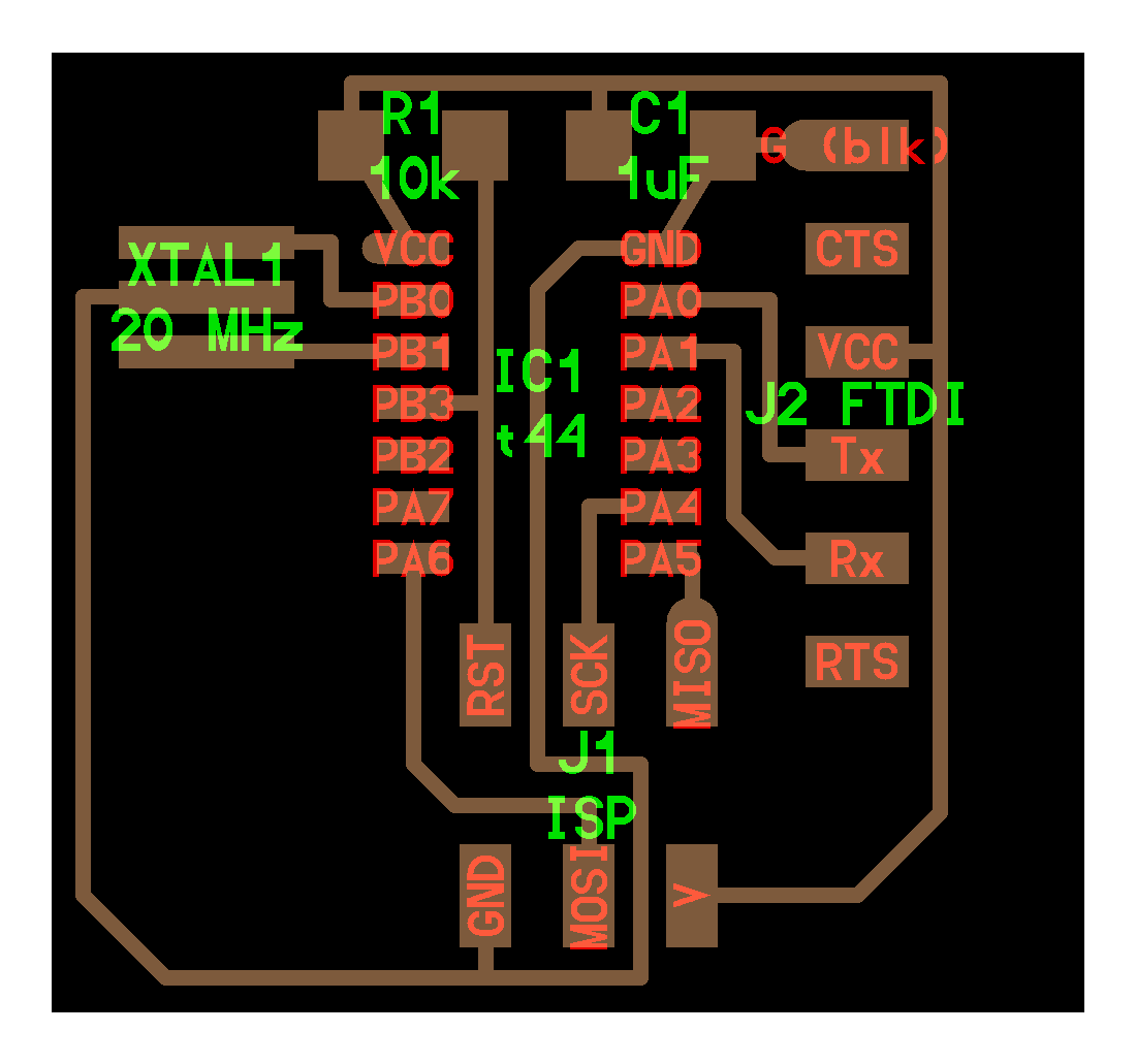
#Electronics design --- This week is about learning how to design a PCB. #### Testing I will do this part when I have access to the lab. Using the test equipment in the lab to observe the operation of a microcontroller circuit board 1. Operating voltage on the board with *multimeter* 2. Use *oscilloscope* to check noise of operating voltage 3. Interpret a data signal using a *logic analyser* If this equipment is not available, another way to test microcontroller circuit boards is by making a simulation in web-apps like [TinkerCAD](https://www.tinkercad.com/) or the open-source Arduino simulator, [Wokwi](https://wokwi.com/). #### Designing I chose a hello.echo board based on ATtiny44 as it has the most available documentation. Here is what the actual board looks like  To add an LED and a switch, I started by making a list of the components required: Components list: 1x ATtiny44 microcontroller 1x 1uF Capacitor 1x header 2x3 1x FTDI connector 1x 10k ohm resistor 1x 20MHz resonator Added components: 1x LED 1x 1kΩ Resistor 1x switch 1x 1kΩ Resistor [Data sheet for ATtiny44](http://ww1.microchip.com/downloads/en/DeviceDoc/Atmel-7701_Automotive-Microcontrollers-ATtiny24-44-84_Datasheet.pdf) Pinout for Attiny44  #### Creating the schematic I used [KiCad 5.1.6](https://kicad-pcb.org/) to design my PCB. KiCad is an open source software suite for Electronic Design Automation (EDA). The program helps create a Schematic in sub-application called Eeschema, and then design the PCB Layout with Gerber output (this is what you send to a manufacturer) in another sub-application called PCBnew. #### Update libraries First step is to import all of the symbol and footprint libraries adapted for SMD components. These libraries can be found [here.](http://academany.fabcloud.io/fabacademy/2020/labs/barcelona/site/local/#material/extras/week06/assets/kicad_libraries.zip)  #### Designing schematic I placed the components listed above one by one, using the place component tool. Then changed properties like annotations and values, by hovering above the component and pressing E which opens the symbol properties window. I also placed some tags using the tag tool - like GND and VCC, to make the schematic neat and clear.  Finally, I generated a Netlist by pressing the green netlist symbol on the toolbar.  However I got an error saying that component R1 did not have footprints defined.  So I went back and assigned footprints to the missing part, by going to its properties again, and selecting the correct footprint from the newly installed libraries. And generated the netlist again.   #### Drawing traces Then I opened the KiCad pcbnew part, and loaded the netlist and stacked of all components in the middle of the board.  Design Rules in KiCAD: To mill the traces we use a 0.4 mm (1/64") end-mill. Which rounds up to 0.016 inches (0.015625 inches) or 16 mil. In the Design Rules Control you can set up Net Classes and Global Design Rules. I change both the trace width and the clearance to 16 mil. I also set the grid size to 16 mil to make it easier.  The components all have an indicative line connection, so I used that to rearrange them and then added the traces, using the trace tool.  After connecting them all, I used the line tool to draw the outline like so.  Next I exported this as svg with these settings:  I opened the svg in Adobe Illustrator, made new layers for the traces and outline respectively.  Then, after checking that the model is in mm, exported both layers separately at 150dpi in png.  #### Creating Toolpaths I followed the same process as [Electronics Production](./Electronics Production.md) week to make toolpaths, mill the board, solder components and test the board. But this time I used [Mods](http://mods.cba.mit.edu/) instead of Fabmodules. Here's the process:  #### At the lab I started to mill the board, solder the components by following the workflow described in [Electronics Production week](./Electronics Production.md). On the first attempt, the I found that the edges of outline were too close to the traces, and they were fragile.  After offsetting the outline farther away, and milling the board again, I found that the pin headers were floating outside instead of resting on the board:  So chaning the outline accordingly, this is how the pins should rest:  And after soldering all components, here is how the final board looks:  Programming and testing of the board is done during the [Embedded Programming](./Embedded Programming.md) week. #### References [Sparkfun KiCad beginners guide](https://learn.sparkfun.com/tutorials/beginners-guide-to-kicad/all) [Reference Documentation](http://archive.fabacademy.org/2016/fablabsingapore/students/98/exercise06.html) #### Design Files [KiCad Schematic](./images/ed/attiny44.sch.zip) [KiCad pcbnew](./images/ed/attiny44.kicad_pcb.zip) [SVG](./images/ed/attiny44-brd.svg) [AI](./images/ed/attiny44-brd.ai.zip) [traces.png](./images/ed/traces.png) [outlines.png](./images/ed/outlines.png) [traces - toolpath for srm20](./images/ed/traces.srm20.rml.zip) [outlines - toolpath for srm20](./images/ed/outlines.srm20.rml.zip)